AD9361,数据接口
CMOSLVDS
CMOS


OSERDESE2为 DDR模式,修改模式为4:1 DDR模式,CLK与CLKDIV为2倍关系。
LVDS


Xilinx原语IBUFDS、OBUFDS
IBUFDS、和OBUFDS都是差分信号缓冲器,用于不同电平接口之间的缓冲和转换。IBUFDS 用于差分输入,OBUFDS用于差分输出。
IBUFDS

https://docs.amd.com/r/en-US/ug953-vivado-7series-libraries/IBUFDS
//   IBUFDS    : In order to incorporate this function into the design,
//   Verilog   : the following instance declaration needs to be placed
//  instance   : in the body of the design code.  The instance name
// declaration : (IBUFDS_inst) and/or the port declarations within the
//    code     : parenthesis may be changed to properly reference and
//             : connect this function to the design.  All inputs
//             : and outputs must be connected.

//  <-----Cut code below this line---->

   // IBUFDS: Differential Input Buffer
   //         Kintex-7
   // Xilinx HDL Language Template, version 2019.1

   IBUFDS #(
      .DIFF_TERM("FALSE"),       // Differential Termination
      .IBUF_LOW_PWR("TRUE"),     // Low power="TRUE", Highest performance="FALSE"
      .IOSTANDARD("DEFAULT")     // Specify the input I/O standard
   ) IBUFDS_inst (
      .O(O),  // Buffer output
      .I(I),  // Diff_p buffer input (connect directly to top-level port)
      .IB(IB) // Diff_n buffer input (connect directly to top-level port)
   );

   // End of IBUFDS_inst instantiation
OBUFDS

https://docs.amd.com/r/en-US/ug953-vivado-7series-libraries/OBUFDS
//     OBUFDS      : In order to incorporate this function into the design,
//     Verilog     : the following instance declaration needs to be placed
//    instance     : in the body of the design code.  The instance name
//   declaration   : (OBUFDS_inst) and/or the port declarations within the
//      code       : parenthesis may be changed to properly reference and
//                 : connect this function to the design.  Delete or comment
//                 : out inputs/outs that are not necessary.

//  <-----Cut code below this line---->

   // OBUFDS: Differential Output Buffer
   //         Kintex-7
   // Xilinx HDL Language Template, version 2019.1

   OBUFDS #(
      .IOSTANDARD("DEFAULT"), // Specify the output I/O standard
      .SLEW("SLOW")           // Specify the output slew rate
   ) OBUFDS_inst (
      .O(O),     // Diff_p output (connect directly to top-level port)
      .OB(OB),   // Diff_n output (connect directly to top-level port)
      .I(I)      // Buffer input
   );

   // End of OBUFDS_inst instantiation
拓展 : IOBUFDS
//     IOBUFDS   : In order to incorporate this function into the design,
//     Verilog   : the following instance declaration needs to be placed
//    instance   : in the body of the design code.  The instance name
//   declaration : (IOBUFDS_inst) and/or the port declarations within the
//      code     : parenthesis may be changed to properly reference and
//               : connect this function to the design.  Delete or comment
//               : out inputs/outs that are not necessary.

//  <-----Cut code below this line---->

   // IOBUFDS: Differential Bi-directional Buffer
   //          Kintex-7
   // Xilinx HDL Language Template, version 2019.1

   IOBUFDS #(
      .DIFF_TERM("FALSE"),     // Differential Termination ("TRUE"/"FALSE")
      .IBUF_LOW_PWR("TRUE"),   // Low Power - "TRUE", High Performance = "FALSE"
      .IOSTANDARD("BLVDS_25"), // Specify the I/O standard
      .SLEW("SLOW")            // Specify the output slew rate
   ) IOBUFDS_inst (
      .O(O),     // Buffer output
      .IO(IO),   // Diff_p inout (connect directly to top-level port)
      .IOB(IOB), // Diff_n inout (connect directly to top-level port)
      .I(I),     // Buffer input
      .T(T)      // 3-state enable input, high=input, low=output
   );

   // End of IOBUFDS_inst instantiation
Xilinx原语 IBUF, OBUF
IBUF
https://docs.amd.com/r/en-US/ug1344-versal-architecture-libraries/IBUF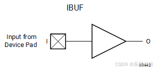
// IBUF: Input Buffer
//       Versal Prime series
// Xilinx HDL Language Template, version 2024.1

IBUF IBUF_inst (
   .O(O), // 1-bit output: Buffer output
   .I(I)  // 1-bit input: Buffer input
);

// End of IBUF_inst instantiation
OBUF
https://docs.amd.com/r/en-US/ug1344-versal-architecture-libraries/OBUF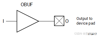
// OBUF: Output Buffer
//       Versal Prime series
// Xilinx HDL Language Template, version 2024.1

OBUF OBUF_inst (
   .O(O), // 1-bit output: Buffer output (connect directly to top-level port)
   .I(I)  // 1-bit input: Buffer input
);

// End of OBUF_inst instantiation
Xilinx原语 IBUFG
IBUFG 通过外部引脚驱动全局时钟网络。
BUFG 通过内部信号驱动全局时钟网络。
Xilinx原语 BUFG,BUFIO,BUFR
BUFG
https://docs.amd.com/r/en-US/ug953-vivado-7series-libraries/BUFG
全局缓冲, BUFG 的输出到达 FPGA 内部的 IOB、 CLB、块 RAM 的时钟延迟和抖动最小.

// BUFG: Global Clock Simple Buffer
//       7 Series
// Xilinx HDL Language Template, version 2024.1

BUFG BUFG_inst (
   .O(O), // 1-bit output: Clock output
   .I(I)  // 1-bit input: Clock input
);

// End of BUFG_inst instantiation
BUFIO
https://docs.amd.com/r/en-US/ug953-vivado-7series-libraries/BUFIO
BUFIO 是 IO 时钟网络,其独立于全局时钟资源,适合采集源同步数据。它只能驱动 IO Block里面的逻辑,不能驱动 CLB 里面的 LUT, REG 等逻辑。
BUFIO 在采集源同步 IO 数据时,提供非常小的延时。但是不能驱动FPGA的内部逻辑,需要BUFIO和BUFG搭配起来使用以实现最佳的性能。
// BUFIO: Local Clock Buffer for I/O
//        7 Series
// Xilinx HDL Language Template, version 2024.1

BUFIO BUFIO_inst (
   .O(O), // 1-bit output: Clock output (connect to I/O clock loads).
   .I(I)  // 1-bit input: Clock input (connect to an IBUF or BUFMR).
);

// End of BUFIO_inst instantiation
BUFR
BUFR 是 regional 时钟网络,它的驱动范围只能局限在一个 clock region 的逻辑。 BUFR 相比 BUFG 的最大优势是偏斜和功耗都比较小。
https://docs.amd.com/r/en-US/ug953-vivado-7series-libraries/BUFR
// BUFR: Regional Clock Buffer for I/O and Logic Resources within a Clock Region
//       7 Series
// Xilinx HDL Language Template, version 2024.1

BUFR #(
   .BUFR_DIVIDE("BYPASS"),   // Values: "BYPASS, 1, 2, 3, 4, 5, 6, 7, 8"
   .SIM_DEVICE("7SERIES")  // Must be set to "7SERIES"
)
BUFR_inst (
   .O(O),     // 1-bit output: Clock output port
   .CE(CE),   // 1-bit input: Active high, clock enable (Divided modes only)
   .CLR(CLR), // 1-bit input: Active high, asynchronous clear (Divided modes only)
   .I(I)      // 1-bit input: Clock buffer input driven by an IBUF, MMCM or local interconnect
);

// End of BUFR_inst instantiation
Xilinx原语 ISERDESE2,OSERDESE2
ISERDESE2
Primitive: Input SERial/DESerializer with Bitslip
// ISERDESE2: Input SERial/DESerializer with Bitslip
//            7 Series
// Xilinx HDL Language Template, version 2024.1

ISERDESE2 #(
   .DATA_RATE("DDR"),           // DDR, SDR
   .DATA_WIDTH(4),              // Parallel data width (2-8,10,14)
   .DYN_CLKDIV_INV_EN("FALSE"), // Enable DYNCLKDIVINVSEL inversion (FALSE, TRUE)
   .DYN_CLK_INV_EN("FALSE"),    // Enable DYNCLKINVSEL inversion (FALSE, TRUE)
   // INIT_Q1 - INIT_Q4: Initial value on the Q outputs (0/1)
   .INIT_Q1(1'b0),
   .INIT_Q2(1'b0),
   .INIT_Q3(1'b0),
   .INIT_Q4(1'b0),
   .INTERFACE_TYPE("MEMORY"),   // MEMORY, MEMORY_DDR3, MEMORY_QDR, NETWORKING, OVERSAMPLE
   .IOBDELAY("NONE"),           // NONE, BOTH, IBUF, IFD
   .NUM_CE(2),                  // Number of clock enables (1,2)
   .OFB_USED("FALSE"),          // Select OFB path (FALSE, TRUE)
   .SERDES_MODE("MASTER"),      // MASTER, SLAVE
   // SRVAL_Q1 - SRVAL_Q4: Q output values when SR is used (0/1)
   .SRVAL_Q1(1'b0),
   .SRVAL_Q2(1'b0),
   .SRVAL_Q3(1'b0),
   .SRVAL_Q4(1'b0)
)
ISERDESE2_inst (
   .O(O),                       // 1-bit output: Combinatorial output
   // Q1 - Q8: 1-bit (each) output: Registered data outputs
   .Q1(Q1),
   .Q2(Q2),
   .Q3(Q3),
   .Q4(Q4),
   .Q5(Q5),
   .Q6(Q6),
   .Q7(Q7),
   .Q8(Q8),
   // SHIFTOUT1, SHIFTOUT2: 1-bit (each) output: Data width expansion output ports
   .SHIFTOUT1(SHIFTOUT1),
   .SHIFTOUT2(SHIFTOUT2),
   .BITSLIP(BITSLIP),           // 1-bit input: The BITSLIP pin performs a Bitslip operation synchronous to
                                // CLKDIV when asserted (active High). Subsequently, the data seen on the Q1
                                // to Q8 output ports will shift, as in a barrel-shifter operation, one
                                // position every time Bitslip is invoked (DDR operation is different from
                                // SDR).

   // CE1, CE2: 1-bit (each) input: Data register clock enable inputs
   .CE1(CE1),
   .CE2(CE2),
   .CLKDIVP(CLKDIVP),           // 1-bit input: TBD
   // Clocks: 1-bit (each) input: ISERDESE2 clock input ports
   .CLK(CLK),                   // 1-bit input: High-speed clock
   .CLKB(CLKB),                 // 1-bit input: High-speed secondary clock
   .CLKDIV(CLKDIV),             // 1-bit input: Divided clock
   .OCLK(OCLK),                 // 1-bit input: High speed output clock used when INTERFACE_TYPE="MEMORY"
   // Dynamic Clock Inversions: 1-bit (each) input: Dynamic clock inversion pins to switch clock polarity
   .DYNCLKDIVSEL(DYNCLKDIVSEL), // 1-bit input: Dynamic CLKDIV inversion
   .DYNCLKSEL(DYNCLKSEL),       // 1-bit input: Dynamic CLK/CLKB inversion
   // Input Data: 1-bit (each) input: ISERDESE2 data input ports
   .D(D),                       // 1-bit input: Data input
   .DDLY(DDLY),                 // 1-bit input: Serial data from IDELAYE2
   .OFB(OFB),                   // 1-bit input: Data feedback from OSERDESE2
   .OCLKB(OCLKB),               // 1-bit input: High speed negative edge output clock
   .RST(RST),                   // 1-bit input: Active high asynchronous reset
   // SHIFTIN1, SHIFTIN2: 1-bit (each) input: Data width expansion input ports
   .SHIFTIN1(SHIFTIN1),
   .SHIFTIN2(SHIFTIN2)
);

// End of ISERDESE2_inst instantiation
OSERDESE2
7系列FPGA器件中的专用并串转换器。
Primitive: Output SERial/DESerializer with bitslip

// OSERDESE2: Output SERial/DESerializer with bitslip
//            7 Series
// Xilinx HDL Language Template, version 2024.1

OSERDESE2 #(
   .DATA_RATE_OQ("DDR"),   // DDR, SDR
   .DATA_RATE_TQ("DDR"),   // DDR, BUF, SDR
   .DATA_WIDTH(4),         // Parallel data width (2-8,10,14)
   .INIT_OQ(1'b0),         // Initial value of OQ output (1'b0,1'b1)
   .INIT_TQ(1'b0),         // Initial value of TQ output (1'b0,1'b1)
   .SERDES_MODE("MASTER"), // MASTER, SLAVE
   .SRVAL_OQ(1'b0),        // OQ output value when SR is used (1'b0,1'b1)
   .SRVAL_TQ(1'b0),        // TQ output value when SR is used (1'b0,1'b1)
   .TBYTE_CTL("FALSE"),    // Enable tristate byte operation (FALSE, TRUE)
   .TBYTE_SRC("FALSE"),    // Tristate byte source (FALSE, TRUE)
   .TRISTATE_WIDTH(4)      // 3-state converter width (1,4)
)
OSERDESE2_inst (
   .OFB(OFB),             // 1-bit output: Feedback path for data
   .OQ(OQ),               // 1-bit output: Data path output
   // SHIFTOUT1 / SHIFTOUT2: 1-bit (each) output: Data output expansion (1-bit each)
   .SHIFTOUT1(SHIFTOUT1),
   .SHIFTOUT2(SHIFTOUT2),
   .TBYTEOUT(TBYTEOUT),   // 1-bit output: Byte group tristate
   .TFB(TFB),             // 1-bit output: 3-state control
   .TQ(TQ),               // 1-bit output: 3-state control
   .CLK(CLK),             // 1-bit input: High speed clock
   .CLKDIV(CLKDIV),       // 1-bit input: Divided clock
   // D1 - D8: 1-bit (each) input: Parallel data inputs (1-bit each)
   .D1(D1),
   .D2(D2),
   .D3(D3),
   .D4(D4),
   .D5(D5),
   .D6(D6),
   .D7(D7),
   .D8(D8),
   .OCE(OCE),             // 1-bit input: Output data clock enable
   .RST(RST),             // 1-bit input: Reset
   // SHIFTIN1 / SHIFTIN2: 1-bit (each) input: Data input expansion (1-bit each)
   .SHIFTIN1(SHIFTIN1),
   .SHIFTIN2(SHIFTIN2),
   // T1 - T4: 1-bit (each) input: Parallel 3-state inputs
   .T1(T1),
   .T2(T2),
   .T3(T3),
   .T4(T4),
   .TBYTEIN(TBYTEIN),     // 1-bit input: Byte group tristate
   .TCE(TCE)              // 1-bit input: 3-state clock enable
);

// End of OSERDESE2_inst instantiation
ad_data_clk
// ***************************************************************************
// ***************************************************************************
// Copyright 2014 - 2017 (c) Analog Devices, Inc. All rights reserved.
//
// In this HDL repository, there are many different and unique modules, consisting
// of various HDL (Verilog or VHDL) components. The individual modules are
// developed independently, and may be accompanied by separate and unique license
// terms.
//
// The user should read each of these license terms, and understand the
// freedoms and responsibilities that he or she has by using this source/core.
//
// This core is distributed in the hope that it will be useful, but WITHOUT ANY
// WARRANTY; without even the implied warranty of MERCHANTABILITY or FITNESS FOR
// A PARTICULAR PURPOSE.
//
// Redistribution and use of source or resulting binaries, with or without modification
// of this file, are permitted under one of the following two license terms:
//
//   1. The GNU General Public License version 2 as published by the
//      Free Software Foundation, which can be found in the top level directory
//      of this repository (LICENSE_GPL2), and also online at:
//      <https://www.gnu.org/licenses/old-licenses/gpl-2.0.html>
//
// OR
//
//   2. An ADI specific BSD license, which can be found in the top level directory
//      of this repository (LICENSE_ADIBSD), and also on-line at:
//      https://github.com/analogdevicesinc/hdl/blob/master/LICENSE_ADIBSD
//      This will allow to generate bit files and not release the source code,
//      as long as it attaches to an ADI device.
//
// ***************************************************************************
// ***************************************************************************

`timescale 1ns/100ps

module ad_data_clk #(

  parameter   SINGLE_ENDED = 0) (

  input               rst,
  output              locked,

  input               clk_in_p,
  input               clk_in_n,
  output              clk);

  // internal signals

  wire                clk_ibuf_s;

  // defaults

  assign locked = 1'b1;

  // instantiations

  generate
  if (SINGLE_ENDED == 1) begin
  IBUFG i_rx_clk_ibuf (
    .I (clk_in_p),
    .O (clk_ibuf_s));
  end else begin
  IBUFGDS i_rx_clk_ibuf (
    .I (clk_in_p),
    .IB (clk_in_n),
    .O (clk_ibuf_s));
  end
  endgenerate

  BUFG i_clk_gbuf (
    .I (clk_ibuf_s),
    .O (clk));

endmodule

// ***************************************************************************
// ***************************************************************************
ad_data_in
// ***************************************************************************
// ***************************************************************************
// Copyright 2014 - 2017 (c) Analog Devices, Inc. All rights reserved.
//
// In this HDL repository, there are many different and unique modules, consisting
// of various HDL (Verilog or VHDL) components. The individual modules are
// developed independently, and may be accompanied by separate and unique license
// terms.
//
// The user should read each of these license terms, and understand the
// freedoms and responsibilities that he or she has by using this source/core.
//
// This core is distributed in the hope that it will be useful, but WITHOUT ANY
// WARRANTY; without even the implied warranty of MERCHANTABILITY or FITNESS FOR
// A PARTICULAR PURPOSE.
//
// Redistribution and use of source or resulting binaries, with or without modification
// of this file, are permitted under one of the following two license terms:
//
//   1. The GNU General Public License version 2 as published by the
//      Free Software Foundation, which can be found in the top level directory
//      of this repository (LICENSE_GPL2), and also online at:
//      <https://www.gnu.org/licenses/old-licenses/gpl-2.0.html>
//
// OR
//
//   2. An ADI specific BSD license, which can be found in the top level directory
//      of this repository (LICENSE_ADIBSD), and also on-line at:
//      https://github.com/analogdevicesinc/hdl/blob/master/LICENSE_ADIBSD
//      This will allow to generate bit files and not release the source code,
//      as long as it attaches to an ADI device.
//
// ***************************************************************************
// ***************************************************************************

`timescale 1ns/100ps

module ad_data_in #(

  // parameters

  parameter   SINGLE_ENDED = 0,
  parameter   FPGA_TECHNOLOGY = 0,
  parameter   IODELAY_ENABLE = 1,
  parameter   IODELAY_CTRL = 0,
  parameter   IODELAY_GROUP = "dev_if_delay_group",
  parameter   REFCLK_FREQUENCY = 200) (

  // data interface

  input               rx_clk,
  input               rx_data_in_p,
  input               rx_data_in_n,
  output              rx_data_p,
  output              rx_data_n,

  // delay-data interface

  input               up_clk,
  input               up_dld,
  input       [ 4:0]  up_dwdata,
  output      [ 4:0]  up_drdata,

  // delay-cntrl interface

  input               delay_clk,
  input               delay_rst,
  output              delay_locked);

  // internal parameters

  localparam  NONE = -1;
  localparam  SEVEN_SERIES = 1;
  localparam  ULTRASCALE = 2;
  localparam  ULTRASCALE_PLUS = 3;

  localparam  IODELAY_CTRL_ENABLED = (IODELAY_ENABLE == 1) ? IODELAY_CTRL : 0;
  localparam  IODELAY_CTRL_SIM_DEVICE = (FPGA_TECHNOLOGY == ULTRASCALE_PLUS) ? "ULTRASCALE" :
    (FPGA_TECHNOLOGY == ULTRASCALE) ? "ULTRASCALE" : "7SERIES";

  localparam  IODELAY_FPGA_TECHNOLOGY = (IODELAY_ENABLE == 1) ? FPGA_TECHNOLOGY : NONE;
  localparam  IODELAY_SIM_DEVICE = (FPGA_TECHNOLOGY == ULTRASCALE_PLUS) ? "ULTRASCALE_PLUS" :
    (FPGA_TECHNOLOGY == ULTRASCALE) ? "ULTRASCALE" : "7SERIES";

  // internal signals

  wire                rx_data_ibuf_s;
  wire                rx_data_idelay_s;
  wire        [ 8:0]  up_drdata_s;

  // delay controller

  generate
  if (IODELAY_CTRL_ENABLED == 0) begin
  assign delay_locked = 1'b1;
  end else begin
  (* IODELAY_GROUP = IODELAY_GROUP *)
  IDELAYCTRL #(.SIM_DEVICE (IODELAY_CTRL_SIM_DEVICE)) i_delay_ctrl (
    .RST (delay_rst),
    .REFCLK (delay_clk),
    .RDY (delay_locked));
  end
  endgenerate

  // receive data interface, ibuf -> idelay -> iddr

  generate
  if (SINGLE_ENDED == 1) begin
  IBUF i_rx_data_ibuf (
    .I (rx_data_in_p),
    .O (rx_data_ibuf_s));
  end else begin
  IBUFDS i_rx_data_ibuf (
    .I (rx_data_in_p),
    .IB (rx_data_in_n),
    .O (rx_data_ibuf_s));
  end
  endgenerate

  // idelay

  generate
  if (IODELAY_FPGA_TECHNOLOGY == SEVEN_SERIES) begin
  (* IODELAY_GROUP = IODELAY_GROUP *)
  IDELAYE2 #(
    .CINVCTRL_SEL ("FALSE"),
    .DELAY_SRC ("IDATAIN"),
    .HIGH_PERFORMANCE_MODE ("FALSE"),
    .IDELAY_TYPE ("VAR_LOAD"),
    .IDELAY_VALUE (0),
    .REFCLK_FREQUENCY (REFCLK_FREQUENCY),
    .PIPE_SEL ("FALSE"),
    .SIGNAL_PATTERN ("DATA"))
  i_rx_data_idelay (
    .CE (1'b0),
    .INC (1'b0),
    .DATAIN (1'b0),
    .LDPIPEEN (1'b0),
    .CINVCTRL (1'b0),
    .REGRST (1'b0),
    .C (up_clk),
    .IDATAIN (rx_data_ibuf_s),
    .DATAOUT (rx_data_idelay_s),
    .LD (up_dld),
    .CNTVALUEIN (up_dwdata),
    .CNTVALUEOUT (up_drdata));
  end
  endgenerate

  generate
  if ((IODELAY_FPGA_TECHNOLOGY == ULTRASCALE) || (IODELAY_FPGA_TECHNOLOGY == ULTRASCALE_PLUS)) begin
  assign up_drdata = up_drdata_s[8:4];
  (* IODELAY_GROUP = IODELAY_GROUP *)
  IDELAYE3 #(
    .SIM_DEVICE (IODELAY_SIM_DEVICE),
    .DELAY_SRC ("IDATAIN"),
    .DELAY_TYPE ("VAR_LOAD"),
    .REFCLK_FREQUENCY (REFCLK_FREQUENCY),
    .DELAY_FORMAT ("COUNT"))
  i_rx_data_idelay (
    .CASC_RETURN (1'b0),
    .CASC_IN (1'b0),
    .CASC_OUT (),
    .CE (1'b0),
    .CLK (up_clk),
    .INC (1'b0),
    .LOAD (up_dld),
    .CNTVALUEIN ({up_dwdata, 4'd0}),
    .CNTVALUEOUT (up_drdata_s),
    .DATAIN (1'b0),
    .IDATAIN (rx_data_ibuf_s),
    .DATAOUT (rx_data_idelay_s),
    .RST (1'b0),
    .EN_VTC (~up_dld));
  end
  endgenerate

  generate
  if (IODELAY_FPGA_TECHNOLOGY == NONE) begin
  assign rx_data_idelay_s = rx_data_ibuf_s;
	assign up_drdata = 5'd0;
  end
  endgenerate

  // iddr

  generate
  if ((FPGA_TECHNOLOGY == ULTRASCALE) || (FPGA_TECHNOLOGY == ULTRASCALE_PLUS)) begin
  IDDRE1 #(.DDR_CLK_EDGE ("SAME_EDGE")) i_rx_data_iddr (
    .R (1'b0),
    .C (rx_clk),
    .CB (~rx_clk),
    .D (rx_data_idelay_s),
    .Q1 (rx_data_p),
    .Q2 (rx_data_n));
  end
  endgenerate

  generate
  if (FPGA_TECHNOLOGY == SEVEN_SERIES) begin
  IDDR #(.DDR_CLK_EDGE ("SAME_EDGE")) i_rx_data_iddr (
    .CE (1'b1),
    .R (1'b0),
    .S (1'b0),
    .C (rx_clk),
    .D (rx_data_idelay_s),
    .Q1 (rx_data_p),
    .Q2 (rx_data_n));
  end
  endgenerate

endmodule

// ***************************************************************************
// ***************************************************************************
ad_data_out
// ***************************************************************************
// ***************************************************************************
// Copyright 2014 - 2017 (c) Analog Devices, Inc. All rights reserved.
//
// In this HDL repository, there are many different and unique modules, consisting
// of various HDL (Verilog or VHDL) components. The individual modules are
// developed independently, and may be accompanied by separate and unique license
// terms.
//
// The user should read each of these license terms, and understand the
// freedoms and responsibilities that he or she has by using this source/core.
//
// This core is distributed in the hope that it will be useful, but WITHOUT ANY
// WARRANTY; without even the implied warranty of MERCHANTABILITY or FITNESS FOR
// A PARTICULAR PURPOSE.
//
// Redistribution and use of source or resulting binaries, with or without modification
// of this file, are permitted under one of the following two license terms:
//
//   1. The GNU General Public License version 2 as published by the
//      Free Software Foundation, which can be found in the top level directory
//      of this repository (LICENSE_GPL2), and also online at:
//      <https://www.gnu.org/licenses/old-licenses/gpl-2.0.html>
//
// OR
//
//   2. An ADI specific BSD license, which can be found in the top level directory
//      of this repository (LICENSE_ADIBSD), and also on-line at:
//      https://github.com/analogdevicesinc/hdl/blob/master/LICENSE_ADIBSD
//      This will allow to generate bit files and not release the source code,
//      as long as it attaches to an ADI device.
//
// ***************************************************************************
// ***************************************************************************

`timescale 1ns/100ps

module ad_data_out #(

  parameter   FPGA_TECHNOLOGY = 0,
  parameter   SINGLE_ENDED = 0,
  parameter   IODELAY_ENABLE = 0,
  parameter   IODELAY_CTRL = 0,
  parameter   IODELAY_GROUP = "dev_if_delay_group",
  parameter   REFCLK_FREQUENCY = 200) (

  // data interface

  input               tx_clk,
  input               tx_data_p,
  input               tx_data_n,
  output              tx_data_out_p,
  output              tx_data_out_n,

  // delay-data interface

  input               up_clk,
  input               up_dld,
  input       [ 4:0]  up_dwdata,
  output      [ 4:0]  up_drdata,

  // delay-cntrl interface

  input               delay_clk,
  input               delay_rst,
  output              delay_locked);

  localparam  NONE = -1;
  localparam  SEVEN_SERIES = 1;
  localparam  ULTRASCALE = 2;
  localparam  ULTRASCALE_PLUS = 3;

  localparam  IODELAY_CTRL_ENABLED = (IODELAY_ENABLE == 1) ? IODELAY_CTRL : 0;
  localparam  IODELAY_CTRL_SIM_DEVICE = (FPGA_TECHNOLOGY == ULTRASCALE_PLUS) ? "ULTRASCALE" :
    (FPGA_TECHNOLOGY == ULTRASCALE) ? "ULTRASCALE" : "7SERIES";

  localparam  IODELAY_FPGA_TECHNOLOGY = (IODELAY_ENABLE == 1) ? FPGA_TECHNOLOGY : NONE;
  localparam  IODELAY_SIM_DEVICE = (FPGA_TECHNOLOGY == ULTRASCALE_PLUS) ? "ULTRASCALE_PLUS_ES1" :
    (FPGA_TECHNOLOGY == ULTRASCALE) ? "ULTRASCALE" : "7SERIES";

  // internal signals

  wire                tx_data_oddr_s;
  wire                tx_data_odelay_s;

  // delay controller

  generate
  if (IODELAY_CTRL_ENABLED == 0) begin
  assign delay_locked = 1'b1;
  end else begin
  (* IODELAY_GROUP = IODELAY_GROUP *)
  IDELAYCTRL #(.SIM_DEVICE (IODELAY_CTRL_SIM_DEVICE)) i_delay_ctrl (
    .RST (delay_rst),
    .REFCLK (delay_clk),
    .RDY (delay_locked));
  end
  endgenerate

  // transmit data interface, oddr -> odelay -> obuf

  generate
  if ((FPGA_TECHNOLOGY == ULTRASCALE) || (FPGA_TECHNOLOGY == ULTRASCALE_PLUS)) begin
  ODDRE1 i_tx_data_oddr (
    .SR (1'b0),
    .C (tx_clk),
    .D1 (tx_data_n),
    .D2 (tx_data_p),
    .Q (tx_data_oddr_s));
  end
  endgenerate

  generate
  if (FPGA_TECHNOLOGY == SEVEN_SERIES) begin
  ODDR #(.DDR_CLK_EDGE ("SAME_EDGE")) i_tx_data_oddr (
    .CE (1'b1),
    .R (1'b0),
    .S (1'b0),
    .C (tx_clk),
    .D1 (tx_data_n),
    .D2 (tx_data_p),
    .Q (tx_data_oddr_s));
  end
  endgenerate

  // odelay

  generate
  if (IODELAY_FPGA_TECHNOLOGY == SEVEN_SERIES) begin
  (* IODELAY_GROUP = IODELAY_GROUP *)
  ODELAYE2 #(
    .CINVCTRL_SEL ("FALSE"),
    .DELAY_SRC ("ODATAIN"),
    .HIGH_PERFORMANCE_MODE ("FALSE"),
    .ODELAY_TYPE ("VAR_LOAD"),
    .ODELAY_VALUE (0),
    .REFCLK_FREQUENCY (REFCLK_FREQUENCY),
    .PIPE_SEL ("FALSE"),
    .SIGNAL_PATTERN ("DATA"))
  i_tx_data_odelay (
    .CE (1'b0),
    .CLKIN (1'b0),
    .INC (1'b0),
    .LDPIPEEN (1'b0),
    .CINVCTRL (1'b0),
    .REGRST (1'b0),
    .C (up_clk),
    .ODATAIN (tx_data_oddr_s),
    .DATAOUT (tx_data_odelay_s),
    .LD (up_dld),
    .CNTVALUEIN (up_dwdata),
    .CNTVALUEOUT (up_drdata));
  end
  endgenerate

  generate
  if (IODELAY_FPGA_TECHNOLOGY == NONE) begin
  assign up_drdata = 5'd0;
  assign tx_data_odelay_s = tx_data_oddr_s;
  end
  endgenerate

  // obuf

  generate
  if (SINGLE_ENDED == 1) begin
  assign tx_data_out_n = 1'b0;
  OBUF i_tx_data_obuf (
    .I (tx_data_odelay_s),
    .O (tx_data_out_p));
  end else begin
  OBUFDS i_tx_data_obuf (
    .I (tx_data_odelay_s),
    .O (tx_data_out_p),
    .OB (tx_data_out_n));
  end
  endgenerate

endmodule

// ***************************************************************************
// ***************************************************************************

DAMO开发者矩阵,由阿里巴巴达摩院和中国互联网协会联合发起,致力于探讨最前沿的技术趋势与应用成果,搭建高质量的交流与分享平台,推动技术创新与产业应用链接,围绕“人工智能与新型计算”构建开放共享的开发者生态。
更多推荐


 3
3 0
0- 0


 已为社区贡献11条内容

所有评论(0)