STM32F407 数据手册不完全要点学习笔记
——
用的是英文原稿,可能写这篇的时候已经出中文了。
STM32F407 数据手册要点摘录
设备摘要/特性
- ARM Cortex-M4 32b MCU+FPU, 210DMIPS
- up to 1MB Flash/192+4KB RAM
- Up to 17 timers:
up to twelve 16-bit and two 32-bit timers up to 168 MHz, each with up to 4
IC/OC/PWM or pulse counter and quadrature(正交) (incremental,增量) encoder input
- 3×12-bit, 2.4 MSPS A/D converters:
up to 24 channels and 7.2 MSPS in triple interleaved mode(三重交替模式)
- 2×12-bit D/A converters
- Up to 140 I/O ports with interrupt capability
– Up to 136 fast I/Os up to 84 MHz
– Up to 138 5 V-tolerant I/Os - 15 communication interfaces :
– Up to 3 × I2C interfaces
– Up to 4 USARTs+2 UARTs
– Up to 3 SPIs (42 Mbits/s)
– 2 × CAN interfaces (2.0B Active)
– SDIO/MMC interface - Ethernet and the camera interface
描述
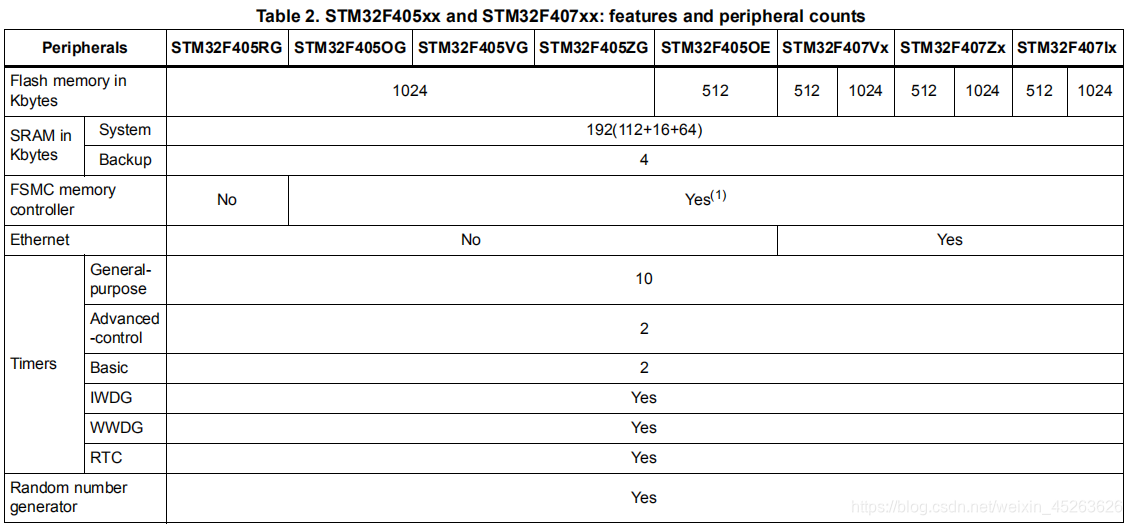
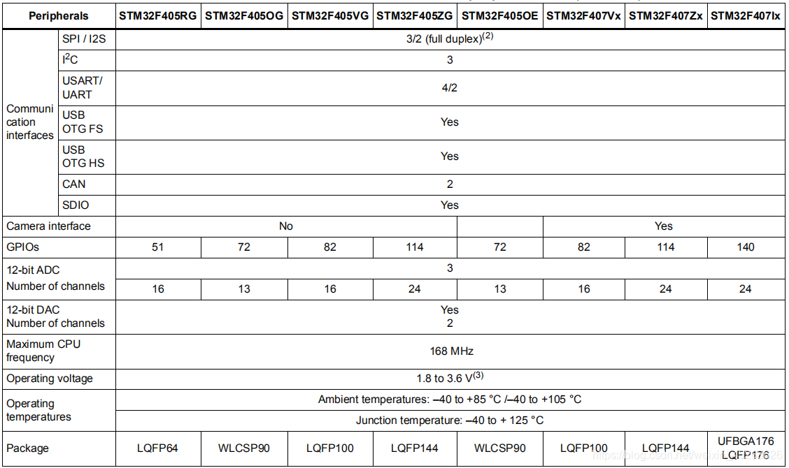
此表引自STMF407X数据手册,2015
Table 2. STM32F405xx and STM32F407xx: features and peripheral counts (continued)
device overview
此处略
引脚排列和引脚说明
FT: 5 V tolerant I/O
Table 7. STM32F40x pin and ball definitions
查看引脚类型、是否为5v容忍引脚
Table 9. Alternate function mapping(复用功能映射)
此表记录了复用功能映射,非常重要,共10页
电气特性
参数条件
Unless otherwise specified:
- all voltages are referenced to VSS.
- typical data are based on TA = 25 °C, VDD = 3.3 V (for the 1.8 V ≤ VDD ≤ 3.6 V voltage range).
绝对最大额定值
Exposure to maximum rating conditions for extended periods may affect
device reliability.
Input voltage on 5v tolerant pin:VSS-0.3~VDD+4V
Input voltage on any other pin:VSS-0.3~4V
工作条件
通用工作条件
VDDA=VDD: 1.8-3.6V
VDDA必须与VDD相连
VREF+:1.8-3.6V
VSSA必须与VREF-相连
VSS必须与VSSA相连
VSS=VSSA=VREF-=GND
VBAT: 1.65-3.6V
——
——
最大结点温度:125℃

DAMO开发者矩阵,由阿里巴巴达摩院和中国互联网协会联合发起,致力于探讨最前沿的技术趋势与应用成果,搭建高质量的交流与分享平台,推动技术创新与产业应用链接,围绕“人工智能与新型计算”构建开放共享的开发者生态。
更多推荐

 1
1 0
0- 0


 已为社区贡献2条内容

所有评论(0)