分析晶圆图像,确定晶圆上芯片(die)之间的距离
分析晶圆图像,通过计算自相关来确定芯片之间的距离
这段代码是使用HALCON软件进行图像处理的脚本,主要用于分析晶圆图像,确定晶圆上芯片(die)之间的距离
dev_update_off ()
read_image (Wafer, ‘wafer/wafer_dies’)
get_image_size (Wafer, Width, Height)
dev_close_window ()
dev_open_window (0, 0, Width, Height, ‘black’, WindowHandle)
dev_set_line_width (2)
set_display_font (WindowHandle, 16, ‘mono’, ‘true’, ‘false’)
dev_display (Wafer)
disp_message (WindowHandle, ‘Determine the size of the dies on the wafer’, ‘window’, 12, 12, ‘black’, ‘true’)
disp_continue_message (WindowHandle, ‘black’, ‘true’)
stop ()
*
- Compute the auto-correlation of the wafer image
rft_generic (Wafer, ImageFFT, ‘to_freq’, ‘n’, ‘complex’, Width)
correlation_fft (ImageFFT, ImageFFT, ImageCorrelation)
rft_generic (ImageCorrelation, ImageFFTInv, ‘from_freq’, ‘n’, ‘real’, Width) - Determine the distance between the dies
local_max_sub_pix (ImageFFTInv, ‘gauss’, 3, 0.0001, Row, Column) - Select indices of neighboring points manually
I0 := 5
I1 := 6
I2 := 9
gen_arrow_contour_xld (Arrow, subset(Row,[I0,I0]), subset(Column,[I0,I0]), subset(Row,[I1,I2]), subset(Column,[I1,I2]), 15, 15)
gen_cross_contour_xld (Cross, Row, Column, 20, rad(45))
distance_pp (Row[I0], Column[I0], Row[I1], Column[I1], DistHor)
distance_pp (Row[I0], Column[I0], Row[I2], Column[I2], DistVert) - Display the results
dev_display (ImageFFTInv)
disp_message (WindowHandle, ‘Auto-correlation of the wafer image…’, ‘image’, 12, 12, ‘black’, ‘true’)
dev_set_color (‘yellow’)
dev_display (Arrow)
disp_message (WindowHandle, DistHor′.2f′+′px′,′image′,Row[I0]−25,(Column[I0]+Column[I1])∗.5−50,′yellow′,′false′)dispmessage(WindowHandle,DistVert'.2f' + ' px', 'image', Row[I0] - 25, (Column[I0] + Column[I1]) * .5 - 50, 'yellow', 'false') disp_message (WindowHandle, DistVert′.2f′+′px′,′image′,Row[I0]−25,(Column[I0]+Column[I1])∗.5−50,′yellow′,′false′)dispmessage(WindowHandle,DistVert’.2f’ + ’ px’, ‘image’, (Row[I2] + Row[I0]) * .5 - 15, Column[I0] - 100, ‘yellow’, ‘false’)
dev_set_color (‘green’)
dev_display (Cross)
disp_continue_message (WindowHandle, ‘black’, ‘true’)
stop () -
- Display the results
dev_display (Wafer)
disp_message (WindowHandle, [‘Auto-correlation of the wafer image…’,‘…corresponds to the die pitch’], ‘image’, 12, 12, ‘black’, ‘true’)
dev_set_color (‘yellow’)
dev_display (Arrow)
disp_message (WindowHandle, DistHor′.2f′+′px′,′image′,Row[I0]−25,(Column[I0]+Column[I1])∗.5−50,′yellow′,′false′)dispmessage(WindowHandle,DistVert'.2f' + ' px', 'image', Row[I0] - 25, (Column[I0] + Column[I1]) * .5 - 50, 'yellow', 'false') disp_message (WindowHandle, DistVert′.2f′+′px′,′image′,Row[I0]−25,(Column[I0]+Column[I1])∗.5−50,′yellow′,′false′)dispmessage(WindowHandle,DistVert’.2f’ + ’ px’, ‘image’, (Row[I2] + Row[I0]) * .5 - 15, Column[I0] - 100, ‘yellow’, ‘false’)
dev_set_color (‘green’)
dev_display (Cross)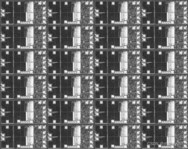
具体步骤和功能如下:
dev_update_off ():关闭窗口的自动更新功能。
read_image (Wafer, ‘wafer/wafer_dies’):读取名为’wafer_dies’的图像文件到变量Wafer中。
get_image_size (Wafer, Width, Height):获取图像的大小,宽度存储在Width,高度存储在Height。
dev_close_window ():关闭当前打开的窗口。
dev_open_window (, , Width, Height, ‘black’, WindowHandle):打开一个新的窗口,窗口大小与图像相同,背景颜色为黑色。
dev_set_line_width (2):设置绘制线条的宽度。
set_display_font (WindowHandle, 16, ‘mono’, ‘true’, ‘false’):设置窗口中显示文字的字体大小、类型等属性。
dev_display (Wafer):在窗口中显示晶圆图像。
disp_message:在窗口中显示提示信息,指导用户确定芯片大小。
stop ():停止执行,等待用户操作。
rft_generic:对晶圆图像进行傅里叶变换,从空间域转换到频率域。
correlation_fft:计算晶圆图像的自相关。
rft_generic:将自相关图像从频率域转换回空间域。
local_max_sub_pix:在自相关图像中寻找局部最大值,这些最大值通常对应于芯片之间的距离。
gen_arrow_contour_xld和gen_cross_contour_xld:生成箭头和十字标记,用于在图像中指示芯片之间的距离。
distance_pp:计算两个点之间的距离。
dev_display:显示自相关图像、箭头和十字标记。
disp_message:在图像中显示芯片水平和垂直方向上的距离。
dev_set_color:设置绘制颜色。
dev_display:再次显示晶圆图像、箭头和十字标记。
disp_message:在图像中显示自相关图像与芯片间距的关系。
上述代码的主要作用是分析晶圆图像,通过计算自相关来确定芯片之间的距离。这对于半导体制造过程中的质量控制和芯片布局分析非常重要。通过在图像中标记芯片间距,可以更直观地评估晶圆的制造质量。

DAMO开发者矩阵,由阿里巴巴达摩院和中国互联网协会联合发起,致力于探讨最前沿的技术趋势与应用成果,搭建高质量的交流与分享平台,推动技术创新与产业应用链接,围绕“人工智能与新型计算”构建开放共享的开发者生态。
更多推荐


 5
5 0
0- 0


 已为社区贡献4条内容

所有评论(0)