半导体芯片生产制造工艺和生产设备全解析:从晶源到一颗芯片的旅程(2/2)
揭秘半导体制造:从晶圆到芯片形成步骤
上一篇我谈到芯片的制造工艺,今天我们将步骤细化,并介绍一些设备
总的流程我们围绕两张流程图来讲
完整版请参考视频: https://www.bilibili.com/video/BV1RDKweMEAP/?vd_source=0fe44b59f009ec279f1191988a29b5d3
上篇传送门:https://zhuanlan.zhihu.com/p/23735296029
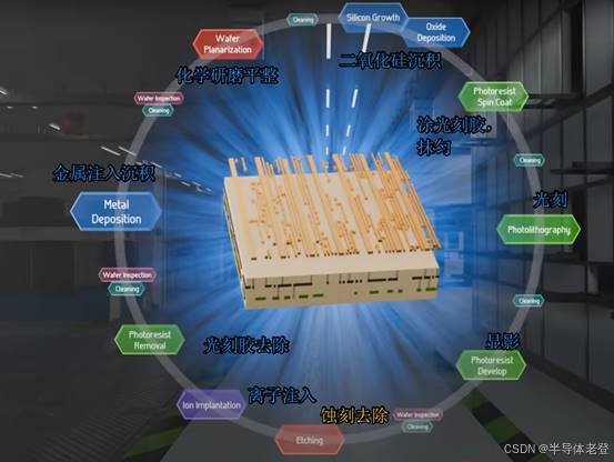
如下面所示:
整体流程是这样
文字流程看下面
- 在晶圆上沉积一层绝缘二氧化硅。
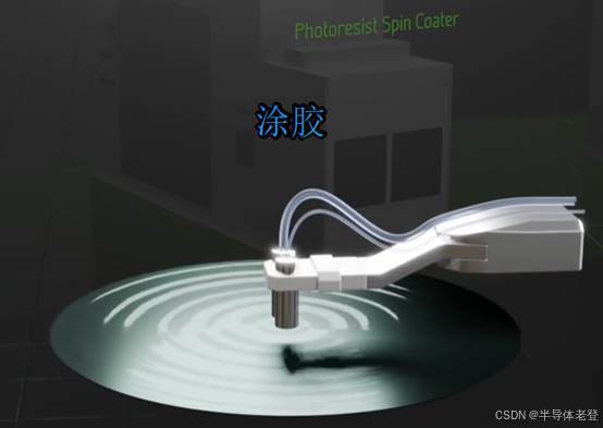
Deposit a layer of insulating silicon dioxide on the wafer. - 在晶圆表面涂上光刻胶,然后进行软烘烤去除溶剂。
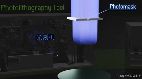
Apply photoresist to the surface of the wafer, and then perform a soft bake to remove the solvent. - 将晶圆通过光刻工具传输,光掩模上的图案通过弱化被光照射到的光刻胶区域转移到晶圆上的每个芯片。
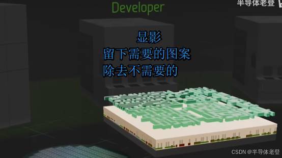
Transfer the wafer through the photolithography tool, and the pattern on the photomask is transferred to each chip on the wafer by weakening the photoresist area exposed to light. - 晶圆进入显影器,洗去被光刻工具光线照射到的部分。
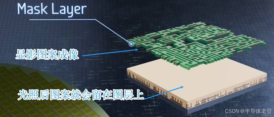
The wafer enters the developer to wash away the part exposed to the light of the photolithography tool. - 对晶圆进行硬烘烤,使剩余的光刻胶变硬,形成掩模层。
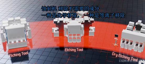
Perform a hard bake on the wafer to harden the remaining photoresist and form a mask layer. - 晶圆进入蚀刻工具,离子蚀刻机通过暴露的二氧化硅去除垂直柱,直到到达前一层的金属容器。
The wafer enters the etching tool, and the ion etcher removes the vertical pillars through the exposed silicon dioxide until it reaches the metal container of the previous layer. - 晶圆被送到光刻胶剥离器,去除掩模层。
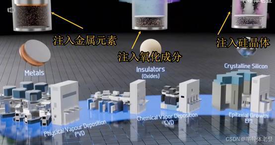
The wafer is sent to the photoresist stripper to remove the mask layer. - 晶圆进入物理蒸汽沉积工具,一系列金属填充暴露的图案并在晶圆上涂上金属。
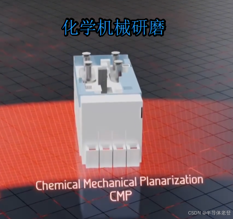
The wafer enters the physical vapor deposition tool, and a series of metals fill the exposed patterns and coat the wafer with metal. - 晶圆被送往化学机械平面化工具,研磨金属,形成平坦的绝缘二氧化硅和与光掩模图案相匹配的导电铜互连。
The wafer is sent to the chemical mechanical planarization tool to grind the metal, forming a flat insulating silicon dioxide and conductive copper interconnections that match the pattern on the photomask.
另外关于离子注入,这个之前也说过,只有在PN层才会用
其他的层进行金属连接是不需要的
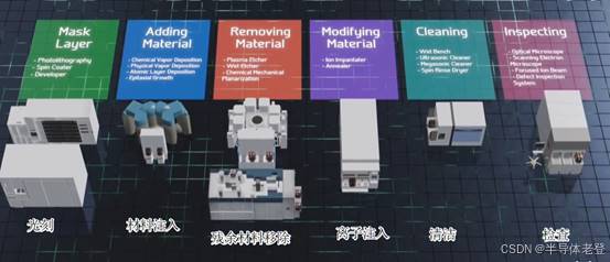
下面我们来细看下流程
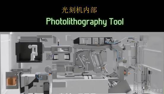
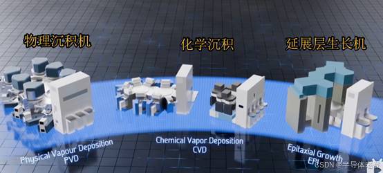
光刻显影相关的设备(photolithography tool.)
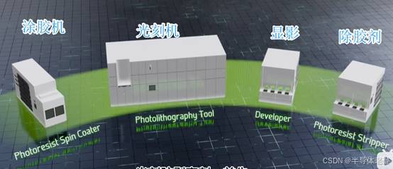
涂胶抹匀
金属注入设备
主要分三类
物理蒸发沉积注入
化学蒸发沉积注入
化学机械平展
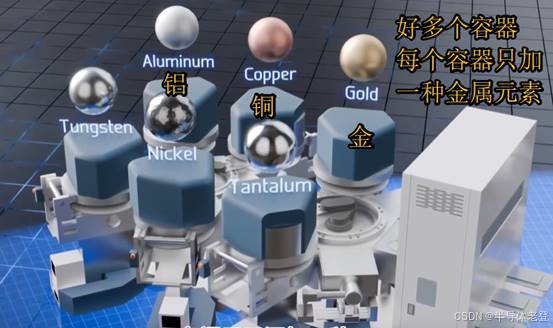
每种元素都放在自己的罐内,
在注入了元素后,有些元素我们不需要的,我们要将他移除
有2中方法
一种是化学移除
一种是高能量等离子移除
这个离子注入只注入P磷和B硼元素,用来形成高掺杂的半岛体,
通俗的说就是根据掺的元素来决定是N型半岛体还是P型半导体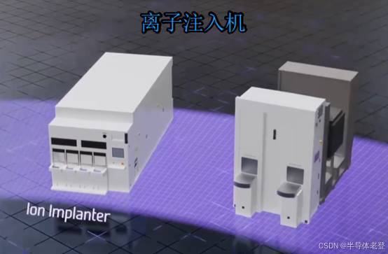
这种和物理方法不一样,此方法直接破坏晶格,如下图所示
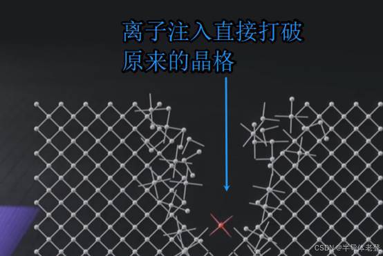
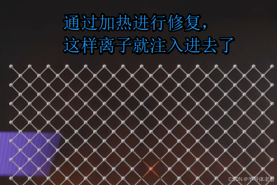
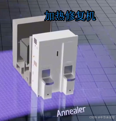
打破了晶格,再注入掺杂元素之后,我们还需修复,一般通过超高温修复
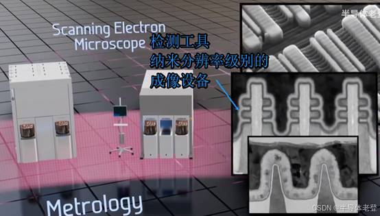
上面基本上说完了所有步骤,清洁的步骤就不说了,
做完后出厂我们要检查的,就用到扫描电子显微镜,分辨率是纳米级别的
通过上面的学习,我想,你基本掌握了晶圆到芯片的工艺过程
有问题请留言交流
喜欢的朋友们可以点赞👍关注 ,谢谢
转载请注明来源 半导体老登

DAMO开发者矩阵,由阿里巴巴达摩院和中国互联网协会联合发起,致力于探讨最前沿的技术趋势与应用成果,搭建高质量的交流与分享平台,推动技术创新与产业应用链接,围绕“人工智能与新型计算”构建开放共享的开发者生态。
更多推荐

 31
31 0
0- 0


 已为社区贡献5条内容

所有评论(0)