AT32F437VM SPI驱动AT7456E OSD芯片
上篇文章讲了BF固件中关于OSD的代码部分,今天来看一下硬件部分。使用AT的芯片配置SPI和OSD芯片通讯。
·
上篇文章讲了BF固件中关于OSD的代码部分,今天来看一下硬件部分。
使用AT的芯片配置SPI和OSD芯片通讯。
先配置一下AT32F437的时钟:
/**
  **************************************************************************
  * @file     at32f435_437_clock.c
  * @brief    system clock config program
  **************************************************************************
  *                       Copyright notice & Disclaimer
  *
  * The software Board Support Package (BSP) that is made available to
  * download from Artery official website is the copyrighted work of Artery.
  * Artery authorizes customers to use, copy, and distribute the BSP
  * software and its related documentation for the purpose of design and
  * development in conjunction with Artery microcontrollers. Use of the
  * software is governed by this copyright notice and the following disclaimer.
  *
  * THIS SOFTWARE IS PROVIDED ON "AS IS" BASIS WITHOUT WARRANTIES,
  * GUARANTEES OR REPRESENTATIONS OF ANY KIND. ARTERY EXPRESSLY DISCLAIMS,
  * TO THE FULLEST EXTENT PERMITTED BY LAW, ALL EXPRESS, IMPLIED OR
  * STATUTORY OR OTHER WARRANTIES, GUARANTEES OR REPRESENTATIONS,
  * INCLUDING BUT NOT LIMITED TO, THE IMPLIED WARRANTIES OF MERCHANTABILITY,
  * FITNESS FOR A PARTICULAR PURPOSE, OR NON-INFRINGEMENT.
  *
  **************************************************************************
  */

/* includes ------------------------------------------------------------------*/
#include "at32f435_437_clock.h"

/**
  * @brief  system clock config program
  * @note   the system clock is configured as follow:
  *         - system clock        = (hext * pll_ns)/(pll_ms * pll_fr)
  *         - system clock source = pll (hext)
  *         - hext                = 8000000
  *         - sclk                = 72000000
  *         - ahbdiv              = 1
  *         - ahbclk              = 72000000
  *         - apb1div             = 2
  *         - apb1clk             = 36000000
  *         - apb2div             = 2
  *         - apb2clk             = 36000000
  *         - pll_ns              = 144
  *         - pll_ms              = 1
  *         - pll_fr              = 16
  * @param  none
  * @retval none
  */
void system_clock_config(void)
{
  /* enable pwc periph clock */
  crm_periph_clock_enable(CRM_PWC_PERIPH_CLOCK, TRUE);

  /* config ldo voltage */
  pwc_ldo_output_voltage_set(PWC_LDO_OUTPUT_1V0);

  /* set the flash clock divider */
  flash_clock_divider_set(FLASH_CLOCK_DIV_2);

  /* reset crm */
  crm_reset();

  /* enable hext */
  crm_clock_source_enable(CRM_CLOCK_SOURCE_HEXT, TRUE);

   /* wait till hext is ready */
  while(crm_hext_stable_wait() == ERROR)
  {
  }

  /* config pll clock resource
  common frequency config list: pll source selected  hick or hext(8mhz)
  _______________________________________________________________________________________
  |        |         |         |         |         |         |         |        |        |
  |pll(mhz)|   288   |   252   |   216   |   180   |   144   |   108   |   72   |   36   |
  |________|_________|_________|_________|_________|_________|_________|_________________|
  |        |         |         |         |         |         |         |        |        |
  |pll_ns  |   72    |   63    |   108   |   90    |   72    |   108   |   72   |   72   |
  |        |         |         |         |         |         |         |        |        |
  |pll_ms  |   1     |   1     |   1     |   1     |   1     |   1     |   1    |   1    |
  |        |         |         |         |         |         |         |        |        |
  |pll_fr  |   FR_2  |   FR_2  |   FR_4  |   FR_4  |   FR_4  |   FR_8  |   FR_8 |   FR_16|
  |________|_________|_________|_________|_________|_________|_________|________|________|

  if pll clock source selects hext with other frequency values, or configure pll to other
  frequency values, please use the at32 new clock  configuration tool for configuration.  */
  crm_pll_config(CRM_PLL_SOURCE_HEXT, 144, 1, CRM_PLL_FR_16);

  /* enable pll */
  crm_clock_source_enable(CRM_CLOCK_SOURCE_PLL, TRUE);

  /* wait till pll is ready */
  while(crm_flag_get(CRM_PLL_STABLE_FLAG) != SET)
  {
  }

  /* config ahbclk */
  crm_ahb_div_set(CRM_AHB_DIV_1);

  /* config apb2clk */
  crm_apb2_div_set(CRM_APB2_DIV_2);

  /* config apb1clk */
  crm_apb1_div_set(CRM_APB1_DIV_2);

  /* select pll as system clock source */
  crm_sysclk_switch(CRM_SCLK_PLL);

  /* wait till pll is used as system clock source */
  while(crm_sysclk_switch_status_get() != CRM_SCLK_PLL)
  {
  }

  /* update system_core_clock global variable */
  system_core_clock_update();
}
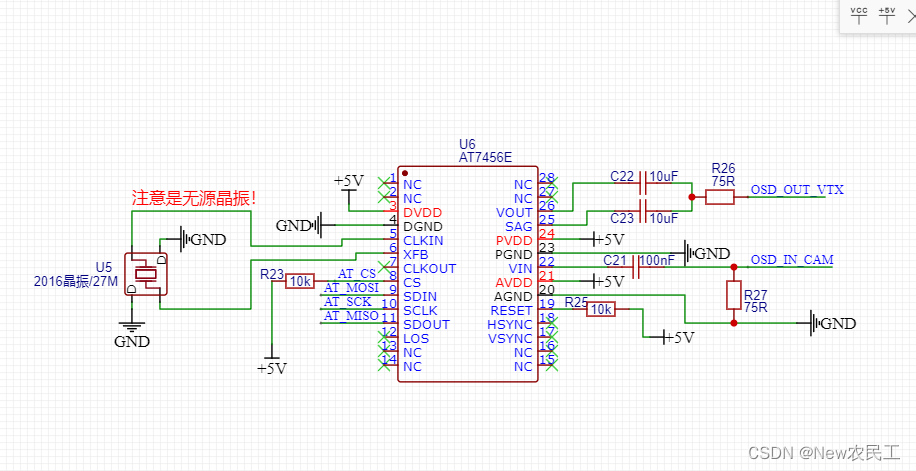
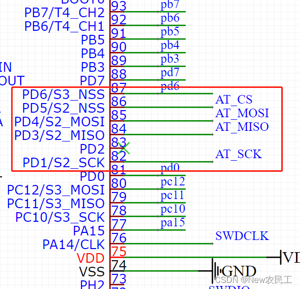
osd芯片连接原理图:
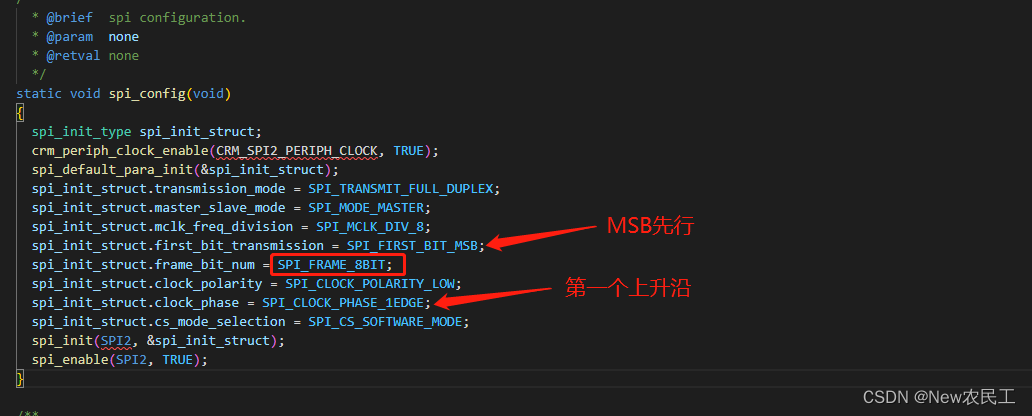
接下来SPI配置:
static void spi_config(void)
{
spi_init_type spi_init_struct;
crm_periph_clock_enable(CRM_SPI2_PERIPH_CLOCK, TRUE);
spi_default_para_init(&spi_init_struct);
spi_init_struct.transmission_mode = SPI_TRANSMIT_FULL_DUPLEX;
spi_init_struct.master_slave_mode = SPI_MODE_MASTER;
spi_init_struct.mclk_freq_division = SPI_MCLK_DIV_8;
spi_init_struct.first_bit_transmission = SPI_FIRST_BIT_MSB;
spi_init_struct.frame_bit_num = SPI_FRAME_8BIT;
spi_init_struct.clock_polarity = SPI_CLOCK_POLARITY_LOW;
spi_init_struct.clock_phase = SPI_CLOCK_PHASE_1EDGE;
spi_init_struct.cs_mode_selection = SPI_CS_SOFTWARE_MODE;
spi_init(SPI2, &spi_init_struct);
spi_enable(SPI2, TRUE);
}
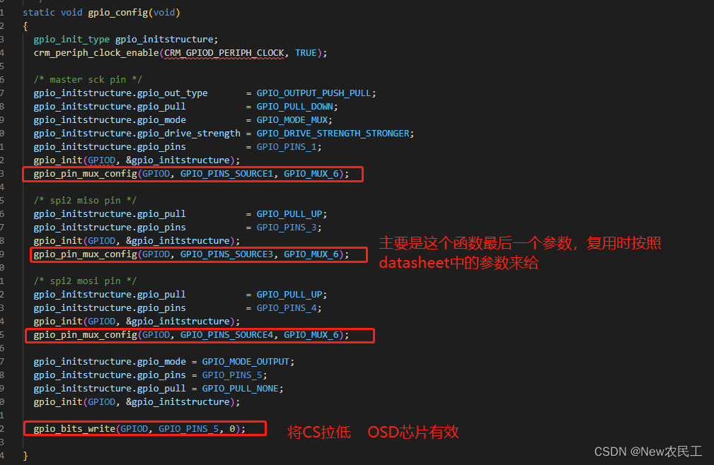
/**
* @brief gpio configuration.
* @param none
* @retval none
*/
static void gpio_config(void)
{
gpio_init_type gpio_initstructure;
crm_periph_clock_enable(CRM_GPIOD_PERIPH_CLOCK, TRUE);
/* master sck pin */
gpio_initstructure.gpio_out_type = GPIO_OUTPUT_PUSH_PULL;
gpio_initstructure.gpio_pull = GPIO_PULL_DOWN;
gpio_initstructure.gpio_mode = GPIO_MODE_MUX;
gpio_initstructure.gpio_drive_strength = GPIO_DRIVE_STRENGTH_STRONGER;
gpio_initstructure.gpio_pins = GPIO_PINS_1;
gpio_init(GPIOD, &gpio_initstructure);
gpio_pin_mux_config(GPIOD, GPIO_PINS_SOURCE1, GPIO_MUX_6);
/* spi2 miso pin */
gpio_initstructure.gpio_pull = GPIO_PULL_UP;
gpio_initstructure.gpio_pins = GPIO_PINS_3;
gpio_init(GPIOD, &gpio_initstructure);
gpio_pin_mux_config(GPIOD, GPIO_PINS_SOURCE3, GPIO_MUX_6);
/* spi2 mosi pin */
gpio_initstructure.gpio_pull = GPIO_PULL_UP;
gpio_initstructure.gpio_pins = GPIO_PINS_4;
gpio_init(GPIOD, &gpio_initstructure);
gpio_pin_mux_config(GPIOD, GPIO_PINS_SOURCE4, GPIO_MUX_6);
gpio_initstructure.gpio_mode = GPIO_MODE_OUTPUT;
gpio_initstructure.gpio_pins = GPIO_PINS_5;
gpio_initstructure.gpio_pull = GPIO_PULL_NONE;
gpio_init(GPIOD, &gpio_initstructure);
gpio_bits_write(GPIOD, GPIO_PINS_5, 0);
}主要注意下面的点
SPI收发函数,因为是全双工模式,所以这里发送和接收在一个函数中。具体可以看上一篇文章说明了为什么要一起做。
/*************************************************************
** Function name:       SPI2SendAndReceviceOneByte
** Descriptions:        使用全双工模式的spi进行发送同时接收一字节数据
** Input parameters:    None
** Output parameters:   None
** Returned value:      None
** Remarks:             None
*************************************************************/
uint8_t SPI2SendAndReceviceOneByte(uint8_t data){
    while(spi_i2s_flag_get(SPI2, SPI_I2S_TDBE_FLAG) == RESET);
    spi_i2s_data_transmit(SPI2, MAX7456ADD_STAT);
    while(spi_i2s_flag_get(SPI2, SPI_I2S_RDBF_FLAG) == RESET);
    return (uint8_t)spi_i2s_data_receive(SPI2);
}
我之前是分开写的,像是下面的样子:发送了两次,接收一次。这样是错误的
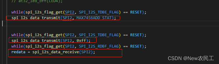
因为第一次是发送数据,所以没接收。但是发现程序只能成功接收一次。
原因:每次发送的同时都会接收数据,如果这次发送完成后,没有将数据读出来。之后的数据就不会覆盖没读出来的数据,导致往后接收失败。
正确写法:
int main(void)
{
  uint16_t redata = 0;
  system_clock_config();
  at32_board_init();
  gpio_config();
  spi_config();

  delay_ms(200);
  SEGGER_RTT_printf(0,"Init ok \r\n");

  while(1)
  {
    SPI2SendAndReceviceOneByte(MAX7456ADD_STAT);
    redata = SPI2SendAndReceviceOneByte(0xff);

    delay_ms(200);
    if (redata != 0){
      SEGGER_RTT_printf(0,"%d   %x\r\n",redata,redata);
    }
    // delay_us(2);
  }
}
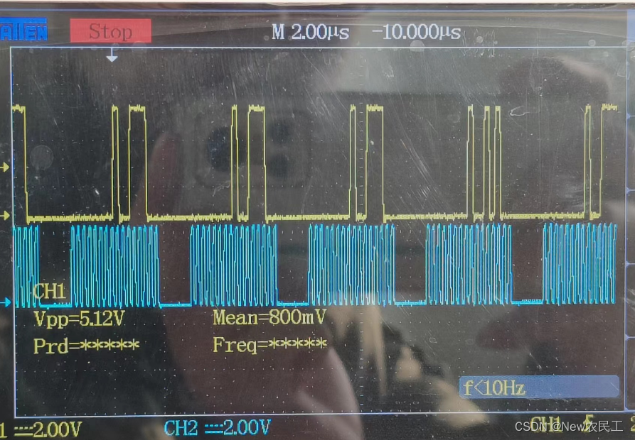
贴个实际的spi信号

DAMO开发者矩阵,由阿里巴巴达摩院和中国互联网协会联合发起,致力于探讨最前沿的技术趋势与应用成果,搭建高质量的交流与分享平台,推动技术创新与产业应用链接,围绕“人工智能与新型计算”构建开放共享的开发者生态。
更多推荐

 1
1 0
0- 0


 已为社区贡献2条内容

所有评论(0)